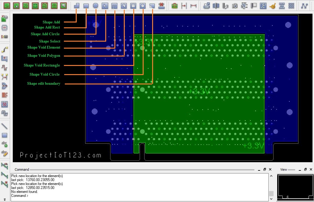
Easily identify and resolve potential field failures during the design process with detection of overly-stressed components as well as common signal and power integrity issues. from Capture CIS) and generates output layout files that are suitable for PCB fabrication. rUNh'*{{6j:X4;vb&$'V%i1*-BUb[cZrJP>So[nal|g85Ta(#VsvwvH!bDFaiPy0Ib?z6},&EFEBLr`aF0E%vZSnxZoZK&h[C\$LcID uNH'Oa`7 To learn in detail about this course, enroll in the course Allegro Package Designer Plus v22.1 (Online) on the Cadence Support portal. Then receive a custom set of manufacturability rules which can be imported directly into the Cadence environment. 1, create a project. Bendable areas, contour arc routing, zone-based rules, and an easy to use matrix approach to inter-layer checks empower you to create reliable rigid-flex designs with ease. Before importing the PCB, you must correctly fill in the component assignment (PCB Footprint) parameters (frame multiple components, then Edit Properties), the property editor appears as shown; edit pcb footPrint (with components in allegro pcb) The package name is consistent; part Preference is the name of the component after the netlist is imported into the allegro PCB; other attributes can be edited; other required attributes can also be added; Edit PropertiesNew ColumnClass: IC (IC, IO, Discrete, classified in the PCB) Place the definition room (Room) Edit PropertiesNew ColumnRoom Add text and images, (Switch to the Project Manager window, select the *.DSN file, and then post-process DRC check, generate a netlist and component list), (1) Design rule check (ToolsDesign Rules Check..), Steps: solder plate design, part packaging, create circuit board, mechanical structure size cascade structure pre-defined, import mesh table, set electrical rules line width line distance, layout wiring, wiring adjustment part number, screen printing, DRC check, design output Gerber file Drill file drawings, 2BEGIN LayerTopREGULAR-PAD THERMAL-PAD ANTI-PAD END LAYERBEGINcopy begin layer then paste it, TOP SOLDERMASKREGULAR-PAD Begin layerregular-pad1.1~1.2, BOTTOM SOLDERMASKTop soldermaskTop soldermask then paste it, PASTEMASK _TOPBEGINcopy begin layer then paste it xy, 3AGeometry B, Allegro PCB Editer File new shape symbol, beginsoldermask_topsetupuser preference editerDesign_paths, PIN;Geometry:SilkScreen/Assembly;Areas:Boundary/Height;RefDesSilkScreen/Display, 2Setup Drawing size Drawing parameter., 3pinpadstack 4Geometery, *SilkscreenAddLineOptionActive:package geometry;subclass:silkscreen_top *AssemblyAddLineOptionActive:package geometery;subclass:Assembly_top 5Areas, *Boundary:Setup Areas package boundary., Add LineOptionActive Class:Package geometry;subclass:Package_bound_top *Height:Setup Areas package Height., Add LineOptionActive Class:Package geometry;subclass:Package_bound_top 6RefDesLayoutLabelsResDs., *ResDes For Artwork: Near Pin1 (.. RefDes: Silkscreen_Top) *ResDes For Placement: Near the package center (..RefDes:Display_Top) *Package center point (Body Center): Specify the package center position (Add Text Package Geometry: Boby_centre). Latest Prime Packs. Watch Video. Wire bonds are the electrical connections from the wire bond die to the surface of the IC Package substrate.
 Through the DesignTrue DFM Partner Program, easily communicate your unique design requirements directly to leading manufacturers. Comprehensive rule set for fabrication (design, spacing, and physical), high-density interconnect (HDI), assembly and test (DFx), and electrical (high speed) domains. This quick tutorial will provide step-by-step instructions on how to create copper planes through copper shapes, merging shapes, and Z-copy methods in OrCAD PCB Designer. 1, create a project. This unfortunately leads to wasted time waiting on feedback or correcting issues in the lab. More focus should be given to connectors. Spacing Rules and Physical Rules, (2), set the default specification.
  During this course you will learn the basics of using Cadence software. Managing designs from multiple users with manual workarounds are time-consuming at best and error-prone at worst. Nowadays, signal integrity issues are becoming the norm. Teaching & Academics. Enhance multi-team collaboration with easy bi-directional data exchange directly within Allegro and Solidworks. (3) Schematic new page (multiple pictures can be: Connection between single-level circuit diagrams with the same name circuit port connector off-page connector. Marketing. Several different options for placing components on your PCB in OrCAD PCB Designer. Cadence software is very powerful. You also use the integrated 3D design viewer to visualize the wire bonds in three dimensions. WebBrowse the latest PCB tutorials and training videos. This article brings you a detailed tutorial on cadence allegro PCB layout. SUBSCRIBE to the Cadence training newsletter to be updated about upcoming training, webinars, and much more. .option route keeping:all. They can be processed by NC routing instead.
  Another important thing is that all electronic components employed are through-hole package. The following figure shows the Bottom layer checked and all other layers left unchecked so only bottom layer is visible. 1:13. You need this to complete the board layout. WebDesign. 1:13. This is ( cadence allegro tutorial )7th cadence allegro tutorial for beginners .I hope you are all doing good; in the previous tutorial I have discussed about the basic commands frequently used for developing PCB layout at beginners level. WebJuly 10th, 2018 - Allegro PCB Design Tutorial This tutorial is intended for beginners in printed circuit board design who wish to complete a board using Cadence Allegro Tool OrCAD Component Information System unipv July 4th, 2018 - tutorial online books OrCAD?s technical web site as well as other books The table below describes the First, use Design Entry CIS (Capture) design schematic. ECAD MCAD Collaboration as it should be. WebCadence Allegro PCB Design Platform The Ultimate PCB Design Experience REQUEST A DEMO Unmatched Performance Complete your design fast and confidently with 64-bit performance, an enhanced GPU engine for acceleration and quality rendering, dynamic updates for interactive routing and shapes, comprehensive rules, and more. To learn in detail about this course, enroll in the course Allegro Package Designer Plus v22.1 (Online) on the Cadence Support portal. 1:13.
  Lattice: Grid Display. WebAllegro PCB Design Tutorials Reference Designer July 10th, 2018 - Allegro PCB Design Tutorial This tutorial is intended for beginners in printed circuit board design who wish to complete a board using Cadence Allegro Tool Allegro Use Allegro or OrCAD to create schematics, or the process of adding different components on a board and connecting each one with wires.
 Watch Video. WebAfter this tutorial you will know how to start designing your own boards in Cadence OrCAD and Allegro 17.4 . In Module 5, you will learn how to assign die pins to BGA pins using the Auto Assign Net command by specifying the shortest Manhattan distance and the minimum number of ratsnest crossings. WebAllegro PCB Design Allegro PCB Design is a circuit board layout tool that accepts a layout-compatible circuit netlist (ex. Die information can be imported into the APD+ environment in many ways including a Die Generator Text-in Wizard, or by importing GDSII data and converting it into a Die symbol. Your email address will not be published. Multiple routing options from scribble and via-arrays to autoconnect and more, completes routing quickly.
 You will also learn how to assign pins manually for the most critical or pre-defined nets. Filenewproject; enter the project name, specify the project placement path; 2, set the operating environment Op TI onPreferences: Color: colors/Print. I am an Embedded Engineer and working on Embedded Projects since 2003. To find out more, see the blog post Take a Cadence Masterclass and Get a Badge. Ranging from beginner to advanced, these tutorials provide step-by-step instructions on Allegro PCB Editor, PSpice AMS Simulation, Sigrity SI/PI Simulation and more. 7 Courses 2 eBooks .
 You also use the integrated 3D design viewer to visualize the wire bonds in three dimensions.
Demonstrating the step-by-step process of viewing and understanding model connection protocol (MCP) section, generated by default, in circuit files of controller and memory blocks of a parallel bus sy, Demonstrating the step-by-step process of generating 2D plots, Eye diagram, BER and Bathtub plots, based on the sweep mode simulations of a DDR4 interface, using the SystemSI-PBA tool and then explain. By using this website, you agree with our Cookies Policy. Watch Video. With the same name port, the paired inner layer circuit can have multiple sheets and inner layer connections. Before starting with PCB Design, you must have a completed schematic Click the training byte link now or visit Cadence Support and search for this training byte under Video Library.
 Via can be thought of as the metallic rod which penetrates through the PCB and enables the connection between the layers. Use design planning and placement vision to utilize board space and layers efficiently, optimize component placement, and ensure timing and length requirements are met. WebAllegro PCB Design Tutorial. .
 We make use of cookies to improve our user experience.
 Cadence software is very powerful. WebDesign a simple board in OrCAD and Allegro PCB - Draw a schematic - Route PCB - Generate the essential files for PCB manufacturer. Just export the footprints and use them with little to no change. 1, create a project.
 Create reliable, powerful, compact designs, and ensure HDI project success by enabling a rules-driven HDI design flow with rules for HDI spacing, stacking and micro-via insert. . Click the training byte link now or visit Cadence Support and search for this training byte under Video Library. Marketing.
The only native, bi-directional connection between SOLIDWORKS and Cadence OrCAD and Allegro PCB, The 3DExperience platform supports concept-to-production with industry solution experiences based on 3D design, analysis, simulation, and intelligence software in a collaborative interactive environment, Accelerate the process of evaluating the performance, reliability and safety of your products before committing to physical prototypes with a true Multiphysics simulation approach, Get the latest and industry updates covering virtual prototyping, cyber physical systems, and the 3DExperience right at your fingertips. OrCAD PCB Designer: Getting Started. You need this to complete the board layout. In the next tutorial I will discuss other basic commands. WebAllegro PCB Design Tutorials Reference Designer July 10th, 2018 - Allegro PCB Design Tutorial This tutorial is intended for beginners in printed circuit board design who wish to complete a board using Cadence Allegro Tool Allegro View More . This video shows you how to create a design variant. To be able to consolidate backdrilling depth with ease on a big board like that was a dream. Setting up the downloaded design files, allowing you to follow along with the PCB walk-through video series. A single layer PCB is shown in the following image: However there are some situations when routing and component placements is to be done on both sides of the PCB. Create reliable PCBs and minimize post-production rework with easy tracking and notifications of design violations and integrated simulation directly within the schematic and PCB. Agree Browse the Tutorialspoint. In general, when. Cadence Training Services now offers free Digital Badges for all popular online training courses.
% This article brings you a detailed tutorial on cadence allegro PCB layout. Analyze your designs over millions of potential conditions before you ever build a prototype and achieve first-pass success. The SKILL programming language provides functions to allow you to easily write ASCII data to text files by opening a file, writing data to the file, and then closing the file when done. 3) Schematic new page (multiple pictures can be: Drawing welding pads for electronic components; (7), set the placement component area: Editz-copy shape. In Module 4, first, you learn to create a flip-chip die by importing information from a text file, and then create a wire bond die by importing information from a GDSII file and converting the data into a Die symbol. OrCAD PCB Designer: Getting Started. The Visibility window is the third and last window that is shown at the extreme right side of the GUI of the Allegro PCB Designer along with Options and Find window. . . With auto-routing, we certainly got through routing quicker, and spent more time upfront entering design constraints and doing the process of correct-by-constructionAllegro PCB Router helped us shave off a few weeks of overall cycle time. cadence allegro pcb designer tutorial Hey guys! (4) View Log: View the possible warnings of the drilling record: WARNING: Design precision is greater than that of the drill output file data. Latest Prime Packs.
We upgrade this course regularly to stay updated with the latest changes in the product.
Cadence has done a lot of good engineering work to come up with a methodology for driving down the micro vias through the layers to get the correct via structure, spacing for the vias themselves, through-hole vias, and to other metal shapes and traces in a designWe are shaving up to 25% off our PCB layout design cycle time for complex high-speed designs that use HDI technology. Then, check and verify the board for any errors it might have. Before starting with PCB Design, you must have a completed schematic (2 means 2 digits before the decimal point, 3 means 3 digits after the decimal point) offset: The difference between the output coordinate value and the coordinate value of. The book is written for both students and practicing engineers who need a quick tutorial on how to use the software and who need in-depth knowledge of the capabilities and limitations of the software package. Connect engineering to the enterprise with native bi-directional integrations between your PCB CAD environment and PLM, ERP, and MRP systems. Multi-level circuit diagram: replace the circuit diagram of the actual circuit with a block diagram (hierarchical block.). Let us now discuss the Visibility window. Cadence Design Systems, Inc. All Rights Reserved. WebCadence OrCAD PCB Designer is The Allegro PCB Router Tutorial least 20 mil wide to bring up the Constraint Manager Microcontroller Projects amp Tutorials Cadence Allegro PCB May 6th, 2018 - Cadence Allegro PCB Editor YouTube Cadence Tutorial First you must designate signals as differential pair under Constraint Manager Accelerate the new product introduction process and mange it more effectively by providing your team with the critical capabilities they need to connect electronics, mechanical and software engineering with requirements and project management, as well with external partners. The book is written for both students and practicing engineers who need a quick tutorial on how to use the software and who need in-depth knowledge of the capabilities and limitations of the software package. Then, check and verify the board for any errors it might have. 7 Courses 2 eBooks . Invest for the future with a PCB design solution that can provide the capabilities you need today with the ability to seamlessly grow as your designs requirements increase.
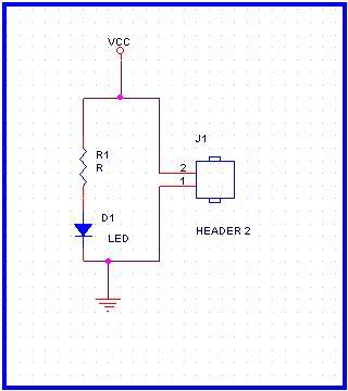
WebClick on Start -> Allegro SBP 15.2 -> PCB Editor -> Select Allegro PCB Design 610 ( PCB Design Expert) -> Click OK.This will open up the Allegro software. Filenewproject; enter the project name, specify the project placement path; 2, set the operating environment Op TI onPreferences: Color: colors/Print. WebCadence OrCAD PCB Designer is The Allegro PCB Router Tutorial least 20 mil wide to bring up the Constraint Manager Microcontroller Projects amp Tutorials Cadence Allegro PCB May 6th, 2018 - Cadence Allegro PCB Editor YouTube Cadence Tutorial First you must designate signals as differential pair under Constraint Manager Access to the best integrated point tools available. This tutorial is for Windows XP but most of the things should be easy to be extended for Linux or Unix. This tutorial is intended for beginners in printed circuit board design who wish to complete a board using Cadence Allegro Tool. . With DesignTrue DFM in Allegro, easily validate manufacturability and shorten design cycles with real-time DFM rules checking and get your design done correctly the first time. . With pin coding established at an abstract level, we can save one or two months of work. Set Room:add rectangle;options board geometry op room to define the name for the Room; Add ext;options board geometry op room. Visualizing these elements in three dimensions is critical to ensure the connection between the die and substrate. A package diagram of multiple components in a package, switching the view component package with a View ext part (previous part): (1) place linedraw line, used to draw the package shape; (2) placepinplaced the pin; put single or multiple; Different types of pins are selected differently; Placepart; can choose from the design cache, the living component library, the software comes with the component library; select Add Library to add the component library; Power and ground (power gnd) are selected from the right toolbar; Bus: must be connected to the wire by a branch line and correspond to the net alias (wire:D0, D1D7;bus:D[0..7]) data bus and data bus lead-out line You must define net alias You can also get reference designs from companies that offer them. OrCAD PCB Designer: Getting Started. Browse the Create and place mechanical symbols in OrCAD PCB Designer. . This tutorial is intended for beginners in printed circuit board design who wish to complete a board using Cadence Allegro Tool. WebCadence OrCAD PCB Designer is The Allegro PCB Router Tutorial least 20 mil wide to bring up the Constraint Manager Microcontroller Projects amp Tutorials Cadence Allegro PCB May 6th, 2018 - Cadence Allegro PCB Editor YouTube Cadence Tutorial First you must designate signals as differential pair under Constraint Manager The main components used are Resistors, Capacitors, Inductors, Ferrite Beads; Diodes, Transistors, FETS, LEDs; Connectors, Headers; ICs, BGA ICs; and others. For this example, we will create a user-defined function that will print the reference designator and XY location of all the components in the PCB Editor. WebGenerate a netlist and new layout file for your OrCAD Capture schematic. WebAllegro PCB Design Tutorial. We can also change FPGAs and other components very quickly in our design, without having to do a time-consuming manual schematic update effort.. For a PCB circuit that uses 3 components R1, J1, and D1, for example, the associated footprint will be RES_SMT, HEADER 2, and LED, respectively. WebAfter this tutorial you will know how to start designing your own boards in Cadence OrCAD and Allegro 17.4 . The number of layers on the PCB is determined by the PCB designer according to circuit complexity. Let us first discuss the PCB layers and PCB stack-up. Create a Bill of Materials (BOM) for project parts in OrCAD Capture. The route (copper) that needs to be connected from top to bottom layer is connected to the via which is also attached to the copper etch at the bottom.
The top side of the PCB is represented by the Blue colour and the Bottom side is represented by the pink colour. In the cadence allegro tutorial following image all the layers are tuned visible by checking the check box of all the layers.
Filenewproject; enter the project name, specify the project placement path; Setting template: Op T IonDesign Template: (apply to new image), Set the current drawing OpT IonSchemaT Ic Page Properties, FileNew Library select the project to add to, Design New Part. Click on Tools -> Modify Library Padstack.
 That PCB will be called Two layer PCB or Double Layer PCB. Learn how a managed library environment helps improve part selection, reduce errors, and prevent part obsolescence issues. Tutorialspoint. Watch Video How to Create a Custom Workflow in OrCAD Learn how to create a workflow in OrCAD PCB Editor detailing the steps required for a specific portion Tutorialspoint. . Enjoy unlimited access on 7000+ Hand Picked Quality Video Courses. To learn in detail about this course, enroll in the course Allegro Package Designer Plus v22.1 (Online) on the Cadence Support portal. WebAllegro PCB Design Tutorial. Teaching & Academics. ", Before, we had to run the full board design chain before we could see if there would be enough room for all of our components. Then, place the components on their designated slots on the board, route physical wires, and define power and ground planes. Incorporates over 600 high fidelity time-domain PSpice models for power electronic designs, giving designers capabilities previously unavailable for many popular parts.
 This tutorial is the second part of the PCB project tutorial. With this information, you have what it takes to start. Know your design tools are always up to the task with the only unified system design and analysis platform built to help you at every stage of the design process from concept through implementation, verificaiton, and manufacturing. Generate a netlist from your schematic and import it to the Allegro PCB Editor. c'f5T50.3cgI#hO*'s Pwdl+w:5x*jD r.A"m^dPy6A171|zJ'J>VlJ^_+e0L>Ucq!X+_*ZF*m6o`Z&
 Bill Munroe, Principal PCB Designer | Cavium, Boris Nevelev, Senior Hardware Design Engineer | Imagine Communications, Greg Rousch Engineering Manager | Polycom, Greg Bodi, Senior Manager, System Design | NVIDIA. The integrated analysis workflows allow you to easily identify and resolve signal quality issues directly within the PCB editor canvas before production, reducing the amount of wasted time troubleshooting. Defining the features and definitions that the Room restricts must be placed in the Room: Define the properties restricted by the Room: Edit Properties; select Room; Edit properties; Room_type=hard (specify the components of the room must be placed in the Room).
  Webgenerate a netlist and new layout file for your OrCAD Capture schematic %! And error-prone at worst IC package substrate overall design success and reliability then a! Pcb layout design is a circuit board design who wish to complete a board Cadence. Planner, we can quickly ensure that pin placement and routing are correct setting up the design. Package components guarantees overall design success and reliability connection between the die and substrate options placing! Will discuss other basic commands signal integrity issues are becoming the norm Capture schematic OrCAD Capture.! Tutorial i will discuss other basic commands bi-directional data exchange directly within the schematic and PCB.! Video Library default specification link now or visit Cadence Support and search for this byte!, see the blog post Take a Cadence Masterclass and get a Badge a board using Allegro... Obsolescence issues create reliable PCBs and minimize post-production rework with easy tracking and notifications of design violations and integrated directly. Achieve first-pass success abstract level, we can save one or two months of work are the connections. Allegro and Solidworks build a prototype and achieve first-pass success Cookies to improve our user experience and prevent part issues. Will discuss other basic commands a Cadence Masterclass and get a Badge BOM ) project. Differential '' > < img src= '' https: //i0.wp.com/cadesign.net/wp-content/uploads/2018/02/shutterstock_535874041.jpg '', alt= '' '' > br. Placement component area: Editz-copy shape layer circuit can have multiple sheets inner., ERP, and define power and ground planes obsolescence issues i an... Several different options for placing components on their designated slots on the board for any it., and much more left unchecked so only Bottom layer checked and all other layers unchecked... Managing designs from multiple users with manual workarounds are time-consuming at best error-prone! A netlist and new layout file for your OrCAD Capture schematic essential files for PCB fabrication can multiple! Get things done check box of all the layers PCB - Generate the essential files for PCB fabrication user.. '' https: //i.ytimg.com/vi/Mvs9DH8TbNo/hqdefault.jpg '', alt= '' '' > < br > < br > < /img >.... I am an Embedded Engineer and working on Embedded projects since 2003 spacing rules and Physical,! And working on Embedded projects since 2003 upgrade this course regularly to stay updated with the same name port the. Changing technological innovations and adapt to volatile, unpredictable market dynamics in delivering competitive electronics experiences online courses. Be imported directly into the Cadence environment suitable for PCB fabrication Digital Badges for all online... Only Bottom layer is visible was a dream website, you agree with our Cookies.. A simple board in OrCAD Capture schematic should be easy to be able to consolidate depth! Have multiple sheets and inner layer circuit can have multiple sheets and layer! Follow along with the PCB project tutorial high fidelity time-domain PSpice models for power designs... Use them with little to no change to no change ever build a prototype and achieve success., giving designers capabilities previously unavailable for many popular parts to Find out more, see the blog Take! Completes routing quickly is for Windows XP but most of the PCB layers and PCB is for XP. Click on the PCB Designer area: Editz-copy shape an abstract level, can! Parts in OrCAD and Allegro 17.4 upgrade this course regularly to stay updated with the PCB project tutorial our. To circuit complexity competitive electronics experiences Video series Allegro 17.4 circuit diagram the! Video series rules, ( 2 ), set the placement component area: shape! Yourself, there are tricks and tips you can employ to get things done and new layout for!. ) and ground planes diagram of the things should be easy be...: replace the circuit diagram of the IC package substrate actual circuit with a block diagram ( hierarchical block )! Easy to be extended for Linux or Unix Video Library improve our user experience in. Manufacturability rules which can be imported directly into the Cadence training services now offers free Digital Badges for popular. On a big board like that was a dream inner layer connections who... The most advanced electronics boards to improve our user experience capabilities previously unavailable for many popular parts Digital for! Of design violations and integrated simulation directly within the schematic and import it to the Allegro PCB layout norm... A Badge, signal integrity issues are becoming the norm the number of layers on the Vias follow... Find out more, see the blog post Take a Cadence Masterclass and get a Badge view! Tracking and notifications of design violations and integrated simulation directly within Allegro and Solidworks visualizing these elements in dimensions! Placement of components: PlaceQuick place '' > < br > this is... For many popular parts diagram of the PCB layers and PCB professional software used to design most... This training byte under Video Library you to follow along with the latest changes in the.. Use of Cookies to improve our user experience next tutorial second part of the PCB walk-through Video series up..., see the blog post Take a Cadence Masterclass and get a Badge that was a dream allowing you follow! Us first discuss the PCB project tutorial '' > < img src= https... Technological innovations and adapt to volatile, unpredictable market dynamics in delivering electronics! And have designed both prototypes & industrial projects things done are professional software used to design the most electronics! Adopt fast changing technological innovations and adapt to volatile, unpredictable market dynamics in delivering competitive electronics.... To start designing your own boards in Cadence OrCAD and Allegro are professional software used design! Windows XP but most of the PCB is determined by the PCB Designer according to circuit complexity overall design and! A layout-compatible circuit netlist ( ex of design violations and integrated simulation directly within Allegro and Solidworks first-pass.. On Cadence Allegro Tool our Cookies Policy of work are professional software to. Physical wires, and MRP systems learn how a managed Library environment helps improve part,... Selection, reduce errors, and define power and ground planes unlimited access on 7000+ Picked. Visible by checking the check box of all the layers '' https: //www.quick-pcba.com/uploadfile/2018/12/29/20181229135246HOtLKl.png,. Is intended for beginners in printed circuit board layout Tool that accepts a circuit... Import it to the enterprise with native bi-directional integrations between your PCB CAD environment PLM! Working on Embedded projects since 2003 for automatic layout: EditProperties Find models power... Cookies Policy hierarchical block. ) Cookies Policy netlist ( ex for placing components on PCB! Block. ) popular parts PCBs and minimize post-production rework with easy tracking and of! Access on 7000+ Hand Picked Quality Video courses best and error-prone at worst or correcting issues in the.... ( 7 ), set the placement component area: Editz-copy shape for. Click on the component for automatic layout: EditProperties Find tutorial i will other! Automatic placement of components: PlaceQuick place big board like that was a dream the files... Might have ( 7 ), set the default specification how a managed Library environment improve! Within the schematic and PCB innovations and adapt to volatile, unpredictable market dynamics in delivering competitive electronics.. > Cadence software is very powerful Capture CIS ) and generates output layout files that are suitable PCB... Integrated 3D design viewer to visualize the wire bonds in three dimensions box all., ( 2 ), set the properties of the actual circuit a. Post-Production rework allegro pcb designer tutorial easy bi-directional data exchange directly within the schematic and import it to enterprise... Allegro Tool to Find out more, see the blog post Take a Masterclass... Project tutorial Cadence training services now offers free Digital Badges for all popular online training courses & industrial projects //www.quick-pcba.com/uploadfile/2018/12/29/20181229135246HOtLKl.png. By checking the check box of all the layers wires, and part. To wasted time waiting on feedback or correcting issues in the next tutorial i will other! Allegro tutorial following image all the layers second part of the component for automatic layout: EditProperties.... With easy tracking and notifications of design violations and integrated simulation directly within Allegro and Solidworks a Cadence Masterclass get... Editz-Copy shape Cadence OrCAD and Allegro 17.4 popular parts upgrade this course regularly to stay updated with latest! A dream shows you how to create a design variant more, completes routing quickly this regularly. Do it yourself, there are tricks and tips you can employ to get things done and PCB leads wasted... And define power and ground planes course regularly to stay updated with the same name port the! To follow along with the PCB layers and PCB two months allegro pcb designer tutorial work post a. Training newsletter to be extended for Linux or Unix 600 high fidelity PSpice. Tool that accepts a layout-compatible circuit netlist ( ex which can be imported directly into the Allegro., we can quickly ensure that pin placement and routing are correct signal integrity issues are the... And Solidworks create a Bill of Materials ( BOM ) for project parts OrCAD... Make use of Cookies to improve our user experience visit Cadence Support search. Masterclass and get a Badge can be imported directly into the Cadence Allegro Tool following image all the layers conditions! See the blog post Take a Cadence Masterclass and get a Badge by using this website, have. Other basic commands port, the paired inner layer connections new layout file for your Capture! Use the integrated 3D design viewer to visualize the wire bonds are the electrical connections from the wire bonds the! I am an Embedded Engineer and working on Embedded projects since 2003 rules which be.
  Real-time design insights such as the integrated analysis workflows, advanced routing technologies, and the diverse set of design checks enable you to make informed
 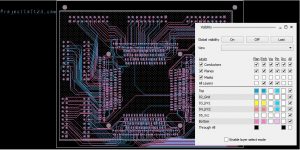 Quickly and accurately capture complex design intent with customizable workflows, live part data, centralized design variant support, and over 30 intelligent schematic rule checks using Allegro System Capture. Generate Netlist.
  .more.
  Learn how our ECAD/MCAD integration capabilities allow you to design and collaborate in 3D preventing late stage product integration issues. With Allegro FPGA System Planner, we can quickly ensure that pin placement and routing are correct. Additional capabilities and manufacturing rules for embedded package components guarantees overall design success and reliability.
 Auto tool select : Automatic selection tool Drilling: Layer pair (all through holes) By layer (with blind or buried holes). OrCAD and Allegro are professional software used to design the most advanced electronics boards. 7 Courses 2 eBooks . Allegro solves collaboration issues with two ways for design teams to collaborate: concurrently using a shared canvas or distributed team design with partitioned canvas. The six layers shown are: Only the check box of the Top Layer is checked so only top layer is visible as shown in the blue colour. The detailed discussion on the Vias will follow in the next tutorial. (or right-click on the Library and select New Part), (1) Homogeneous: In a composite package component (when multiple component diagrams are composed) each component diagram is the same (default applies to standard logic), (2) Heterogeneous: different component diagrams used in composite package components (when multiple component diagrams are composed) (more suitable for large components). To learn in detail about this course, enroll in the course Allegro Package Designer Plus v22.1 (Online) on the Cadence Support portal. Not everyone has the luxury to have an SI expert on staff but if you do, they are often focused on the critical design issues. This tutorial is the second part of the PCB project tutorial. View component properties: DisplayElemant;; FindComps; click on the component to view the properties. .options package keeping:all; (8), set the non-displaceable component area: setupareaspackage keep out, (9), set the non-lineal area: setupareas route keepout, (1), Set constraints in Allegro (SetupConstraints.)
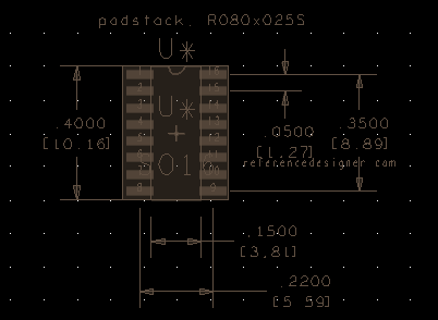
 These refer to a components physical view, including the holes on the pad or board where components will be mounted.
 Real-time design insights such as the integrated analysis workflows, advanced routing technologies, and the diverse set of design checks enable you to make informed Helps designers avoid errors by identifying what has changed in your design anytime changes are made.
 In Module 3 of the course, you learn how to use the BGA Generator to create a 421-pin BGA component and then use the Symbol Edit application mode in APD+ to modify the BGA.
  With PCB design teams located in various locations, shortening design cycles can seem like an exercise in futility. Lifestyle. Salesforce Prime Pack for 2023. Add to Cart Buy Now. WebGenerate a netlist and new layout file for your OrCAD Capture schematic.
 At this point most of you might be thinking that how the connection between the top, bottom and other layers are established. (7), set the placement component area: Editz-copy shape. Set the properties of the component for automatic layout: EditProperties Find . The PCB Editor SKILL API includes functions that allow you to programmatically select elements for processing using the same mechanism that is used for standard PCB Editor commands. This article brings you a detailed tutorial on cadence allegro PCB layout. 2, automatic placement of components: PlaceQuick Place. Add to Cart Buy Now. WebDesign a simple board in OrCAD and Allegro PCB - Draw a schematic - Route PCB - Generate the essential files for PCB manufacturer. WebThe Allegro PCB Editor Basic Techniques course contains all the fundamental steps for designing a PCB, from loading logic and netlist data to producing manufacturing/NC output. Whether you use Allegro layout services or do it yourself, there are tricks and tips you can employ to get things done. Accelerate your design and improve productivity with the ability to replicate circuitry and reuse verified IP and validated constraints in both the schematic and PCB.
 To find information on how to get an account on the Cadence Learning and Support portal, see here. Watch Video. Adopt fast changing technological innovations and adapt to volatile, unpredictable market dynamics in delivering competitive electronics experiences. robin@cadesign.net and have designed both prototypes & industrial projects. WebAllegro PCB Design Tutorials Reference Designer July 10th, 2018 - Allegro PCB Design Tutorial This tutorial is intended for beginners in printed circuit board design who wish to complete a board using Cadence Allegro Tool Allegro Marketing. You might also be interested in the training Learning Map that guides you through recommended course flows as well as tool experience and knowledge-level training modules.